FIL-ASIC Roadmap —The World's First Sovereign AI Chip.

A 5nm chip built on algebra, manufactured on sovereign soil.

Why a Custom ASIC

The G1 PCIe card brings FIL computation to market rapidly using FPGA and optimised ASIC components. It is a powerful, deployable product. But it is not the endgame.

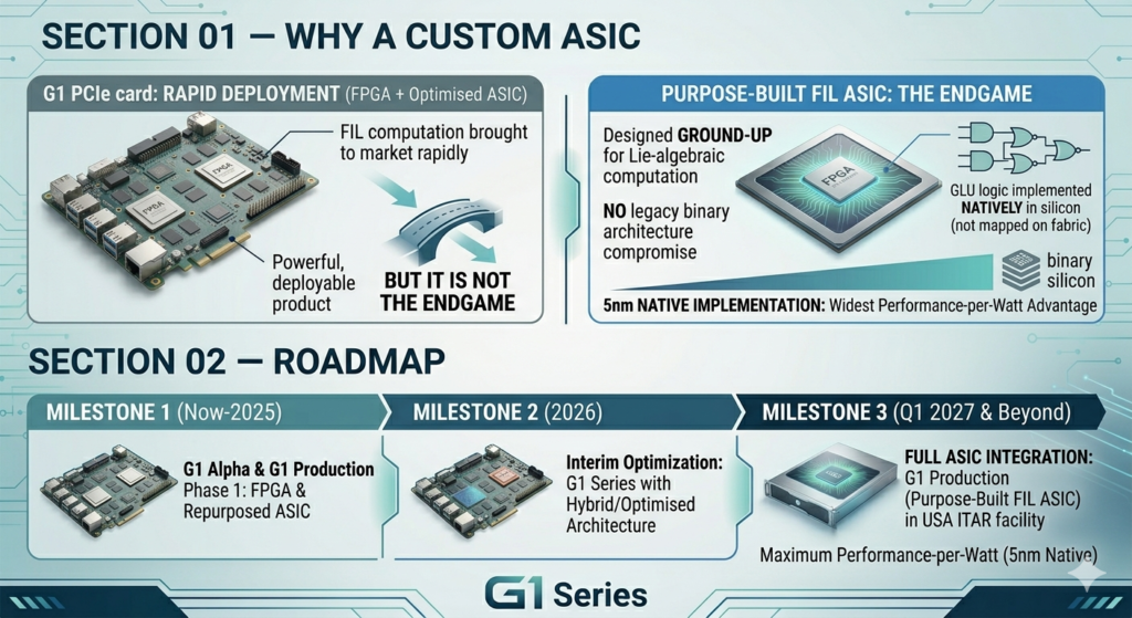
A purpose-built FIL ASIC — designed ground-up for Lie-algebraic computation, without any legacy binary architecture compromise — will deliver the full performance and efficiency potential of the FIL framework. At 5nm, with GLU logic implemented natively in silicon rather than mapped onto general-purpose programmable fabric, the performance-per-watt advantage over binary silicon will be at its widest.

Roadmap

Milestone Table
Milestone Detail
Q2 2026 — G1 Alpha ✓ FPGA validation complete. FIL/GLU architecture verified on Xilinx Ultrascale+ fabric. Benchmark data collected and under NDA review by partners.
Q4 2026 — G1 Production First production-grade G1 cards manufactured at Aterna's ITAR compliant USA facility. Initial allocation to sovereign government and enterprise partners.
Q4 2027 — FIL-ASIC Tape-out 5nm FIL-ASIC tape-out. First purpose-built Lie-algebraic compute chip. Designed on 100% Aterna original IP. Manufactured under ITAR-compliant protocols.
2028 — Saudi Arabia Fab Bridge Strategic manufacturing scale-up with Kingdom of Saudi Arabia partners. Local production capability within the Kingdom.

What the ASIC Changes

The FIL-ASIC is not simply a faster G1. It is the materialisation of silicon sovereignty. A compute chip designed in full, manufactured without foreign IP licensing, and producible within a partner nation’s borders represents a qualitatively different class of strategic asset. It is the difference between deploying foreign hardware with friendly intent, and owning the means of computation.

...

Fill out the form to request the document